Understanding the basic memory architecture of whatever system you’re programming for is necessary to create high performance applications. Most desktop systems consist of large amounts of system memory connected to a single CPU, which may have 2 or three levels or fully coherent cache. Before you get started with CUDA, you should read this to understand the basic memory hierarchy of modern CUDA capable compute devices.
Why memory and cache architecture is important
Most programming courses in college focus on basic algorithms and data structures, but ignore cache and memory structure altogether. Unfortunately, understanding how the memory hierarchy and cache structure work is vital to achieving high performance. In the image processing with SSE article, I show two functions which perform a quick calculation to each pixel in an image, RemoveBlue, and RemoveBlue2. RemoveBlue processed pixels from top to bottom, left to right, and finished in 6.7 milliseconds. RemoveBlue2 processed pixels from left to right, top to bottom, and finished in 0.54 milliseconds. Because RemoveBlue2 processed pixels in a cache friendly manner, the function executes over 12 times as fast as the non-cache friendly function. Similar phenomenon can also be experienced on GPUs if the cache isn’t used properly.
 Basic Memory Hierarchy
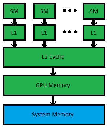
Below is a basic diagram of the memory structure in a modern system using nVidia’s Fermi architecture. Note that the GPU has its own memory on board. On mid to high end workstations, this can be anywhere from 768 megabytes all the way up to 6 gigabytes of GDDR5 memory. Typical system memory for computers nowadays ranges anywhere from 6 gigs to 64 gigs or more of DDR3 memory for the highest end workstations. In short, GPUs don’t have as much memory, but the memory bandwidth for GPUs is usually substantially higher than that of even the highest end Intel or AMD CPUs.
All modern CUDA capable cards (Fermi architecture and later) have a fully coherent L2 Cache. As with memory, the GPU’s L2 cache is much smaller than a typical CPU’s L2 or L3 cache, but has much higher bandwidth available. Having this L2 cache is terrific for compute applications such as raytracing, where memory access patterns are very complex and random.
Finally, the L1 cache onboard a GPU is smaller than L1 cache in a CPU, but again, it has much higher bandwidth. High end nVidia graphics cards have several streaming multiprocessors, or SMs, each is equipped with its own L1 cache. Unlike most high end CPUs which have 4 or 6 cores, high performance CUDA GPUs have 16 SMs. It is very important to note that unlike CPU architectures from Intel and AMD, the L1 caches in CUDA capable cards are not coherent. This means that if two different SMs are reading and writing to the ‘same’ memory location, there is no guarantee that one SM will immediately see the changes from the other SM. These sorts of problems are difficult to debug, so you need to think carefully whenever you want two different threads from different thread blocks manipulating the same piece of memory.
Typical high end workstation memory and cache
| CPU | GPU | |
| Memory | 6 -> 64 GB | 768MB -> 6 GB |
| Memory Bandwidth | 24 -> 32 GB/s | 100 -> 200 GB/s |
| L2 Cache | 8 -> 15 MB | 512 -> 768 kB |
| L1 Cache | 256 -> 512 kB | 16 -> 48 kB |
Memory Coalescing
One word that you won’t hear much in CPU programming is memory coalescing. In CUDA, you typically have 32 threads working together in unison. So many times, you have 32 threads, each wanting to write a 32-bit result to the main GPU memory. In order to accomplish this task with an absolute minimal number of memory transactions, its best if the memory accesses are coalesced such that there are no bank conflicts. It’s actually a little difficult to describe with words. Because memory coalescing is so important for achieving high GPU performance, I encourage you to take a look at the latest CUDA Programming Guide, where there are many easy to understand pictures explaining memory coalescing.